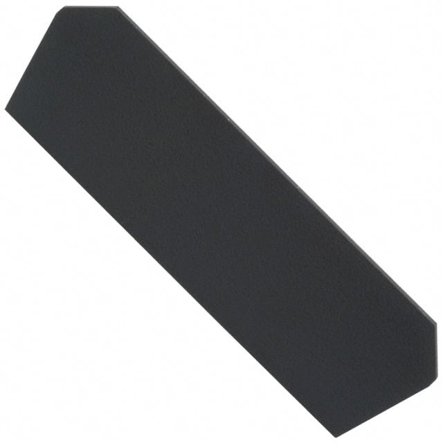
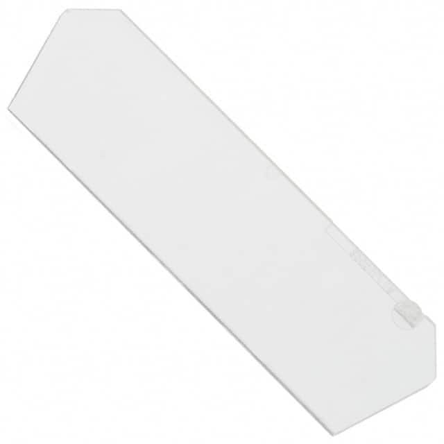
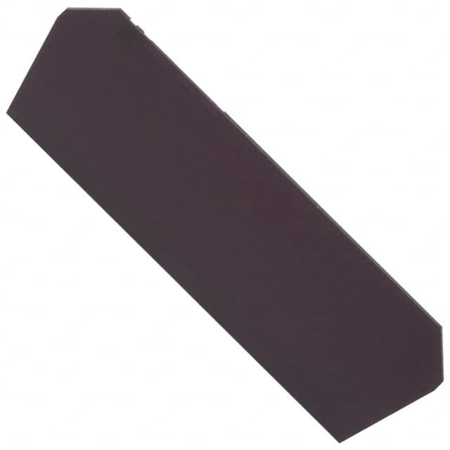
2003 Microsemi Corporation TRANS HBT RF BIPOLAR 55BT
Дискретті жартылай өткізгіштер
Өндіруші нөмірі:
2003
Өндіруші:
Өнім санаты:
Сипаттамасы:
TRANS HBT RF BIPOLAR 55BT
RoHs күйі:
Деректер кестелері:
Бөлім күйі :
Obsolete
Жабдықтаушы құрылғы пакеті :
55BT-1
Жиілік - Өту :
2GHz
Жұмыс температурасы :
200°C (TJ)
Кернеу - коллектор эмиттерінің бұзылуы (макс.) :
50V
Монтаждау түрі :
Chassis Mount
Пакет/қорап :
55BT-1
Сериялар :
-
Табыс :
8.5dB
Ток - коллектор (Ic) (макс.) :
500mA
Транзистор түрі :
NPN
Тұрақты токтың өсуі (hFE) (мин) @ Ic, Vce :
10 @ 100mA, 5V
Шу көрсеткіші (дБ Typ @ f) :
-
Қаптама :
Bulk
Қуат - Макс :
12W
Қоймада
45,439
Unit Price:
Бізбен байланысыңыз ұсыныс
2003 Конкурентные цены
ChipIc бірегей жабдықтау көзі бар. Біз 2003 қосымшасын ұсына аламыз
біздің клиенттер үшін бәсекеге қабілетті баға. Сіз біздің ең жақсысынан ләззат ала аласыз
Chipmlcc 2003 сатып алу арқылы қызмет көрсету. қатысты бізге хабарласыңыз
2003 сайтындағы ең жақсы баға. Ұсыныс алу үшін басыңыз
2003 Особенности
2003 is produced by Microsemi Corporation, belongs to Транзисторлар - Биполярлы (BJT) - RF.
2003 Өнім туралы мәліметтер
:
2003 — Транзисторлар - Биполярлы (BJT) - RF буферлік күшейткіштер әзірленген және
өндірілген
Microsemi Corporation.
Microsemi Corporation ұсынған 2003 файлын CHIPMLCC сайтынан сатып алуға болады.
Мұнда жетекші өндірушілердің әртүрлі электронды бөлшектерін таба аласыз бейбітшілік.
CHIPMLCC 2003 сапасы қатаң бақылаудан өтіп, сәйкес келеді барлығы талаптар.
CHIPMLCC-те көрсетілген қор күйі тек анықтама үшін берілген.
Егер сіз іздеген бөлікті таппасаңыз, бізбен байланыса аласыз деректер кестесіндегі қорлардың саны сияқты қосымша ақпарат 2003 (PDF), бағасы 2003, Pinout 2003, нұсқаулық 2003 Және 2003 ауыстыру шешімі.
2003 FAQ
:
1. Q: What is the difference between a diode and a transistor?
A: A diode is a two-terminal electronic component that allows current to flow in one direction only, while a transistor is a three-terminal device used for amplification and switching purposes.
2. Q: How does a semiconductor work as a conductor?
A: Semiconductors can conduct electricity under certain conditions due to their ability to change from insulating to conducting state when exposed to an electric field or light.
3. Q: What are the main challenges in fabricating high-quality silicon wafers?
A: The main challenges in fabricating high-quality silicon wafers include controlling impurities, achieving uniform crystal structure, and minimizing defects during the manufacturing process.
4. Q: Can you explain the concept of doping in semiconductors?
A: Doping involves intentionally introducing impurities into a semiconductor to alter its electrical properties, such as creating n-type or p-type regions to control conductivity.
5. Q: What are the key differences between CMOS and bipolar transistors?
A: CMOS transistors consume less power and have higher noise immunity compared to bipolar transistors, making them suitable for integrated circuits with low power requirements.
6. Q: How do photolithography techniques contribute to semiconductor manufacturing?
A: Photolithography is used to transfer patterns onto semiconductor wafers, allowing for precise etching and deposition processes to create intricate circuitry and components.
7. Q: What role does the cleanroom environment play in semiconductor fabrication?
A: Cleanrooms provide a controlled environment with low levels of airborne particles to prevent contamination during the delicate processes involved in semiconductor fabrication.
8. Q: Can you explain the concept of electron mobility in semiconductors?
A: Electron mobility refers to the speed at which electrons move through a semiconductor material under the influence of an electric field, impacting the material's overall conductivity.
9. Q: What are the primary methods for testing the quality and performance of semiconductor devices?
A: Semiconductor devices are typically tested using techniques such as electrical characterization, reliability testing, and failure analysis to ensure their functionality and durability.
10. Q: How do advancements in semiconductor technology impact the development of electronic devices?
A: Advancements in semiconductor technology enable the creation of smaller, more efficient, and higher-performing electronic devices, driving innovation across various industries.
2003 Қатысты кілт сөздер
:
2003 Бағасы
2003 Кескіндеме
2003 Істік кернеу
Науқандар: Жылдам дәйексөзді тексеру
Ең аз тапсырыс: 1
Contains
"2003"
series
products